
Contents
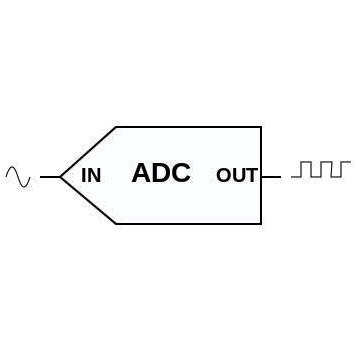
In this tutorial we will learn, how to use the ADC module of a PIC Microcontroller using MPLAB XC8 compiler. For demonstration we will use the commonly available PIC 16F877A microcontroller.
Every physical quantity found in nature like temperature, humidity, pressure, force is analog. We need to convert these analog quantities to digital to process it using a digital computer or a microcontroller. This is done by using Analog to Digital Converters. An Analog to Digital Converter or ADC is a device which converts continuous analog quantity (here : voltage) to corresponding discrete digital values.
PIC 16F877A microcontroller has 8 ADC inputs and it will convert analog inputs to a corresponding 10 bit digital number. For the sake of explanation take ADC Lower Reference as 0V and Higher Reference as 5V.
- Vref- = 0V
- Vref+ = 5V
- n = 10 bits
- Resolution = (Vref+ – Vref-)/(2n – 1) = 5/1023 = 0.004887V
So ADC resolution is 0.00487V, which is the minimum required voltage to change a bit. See the examples below.
| Analog Input | Digital Output | ||
|---|---|---|---|
| Binary | Hex | Decimal | |
| 0 | 0b0000000000 | 0x000 | 0 |
| 0.004887V | 0b0000000001 | 0x001 | 1 |
| 0.009774V | 0b0000000010 | 0x002 | 2 |
| 0.014661V | 0b0000000011 | 0x003 | 3 |
| 4.999401V | 0b1111111111 | 0x3FF | 1023 |
The ADC module of PIC 16F877A has 4 registers.
- ADRESH – A/D Result High Register
- ADRESL – A/D Result Low Register
- ADCON0 – A/D Control Register 0
- ADCON1 – A/D Control Register 1
ADC Block Diagram
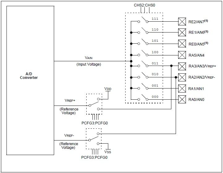
From this block diagram you can easily understand the working of ADC channel selection and reference voltage selection.
ADCON0 – A/D Control Register 0
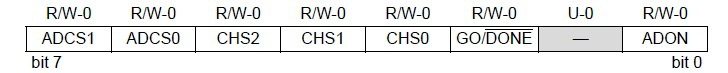
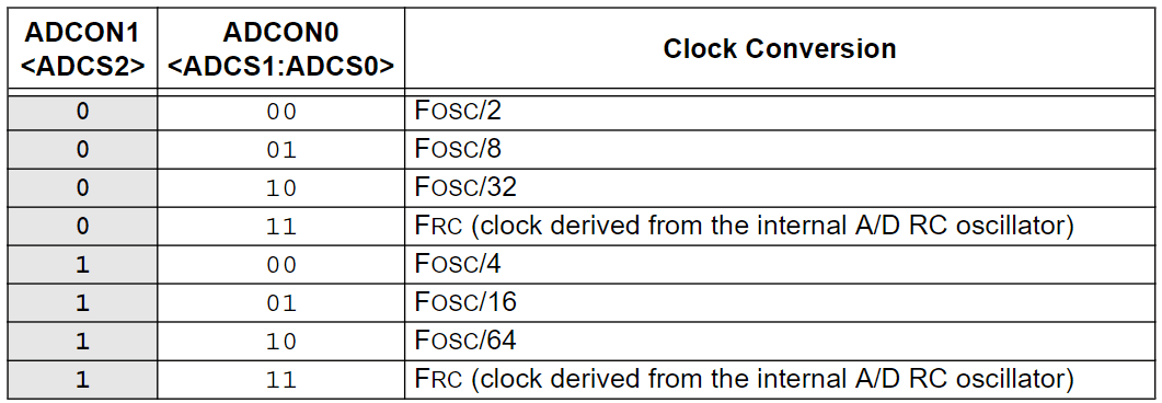
- Bit 7 ~ 6 : ADCS1 & ADCS0, A/D Conversion clock selection bits. These bits are used in combination with ADCS2 of ADCON1 register. (See the ADC Clock Selection Table)
- Bit 5 ~ 3 : CH2, CH1 & CH0 are analog channel selection bits which will select a particular channel out of 8.
- Bit 2 : Go_nDone is the A/D conversion status bit. Setting this bit initiates the A/D conversion and it will be automatically cleared when the conversion completes.
- Bit 1 : Unimplemented, Read as 0.
- Bit 0 : ADON, A/D Module On bit. Setting this bit will turn on the ADC module.
ADCON1 – A/D Control Register 1
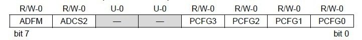
- Bit 7 : ADFM, A/D Result Format bit. Bits of result will be right justified if this bit is set otherwise it will be left justified.
- Bit 6 : ADCS2, A/D Conversion clock selection bit. This bit is used in combination with ADCS0 and ADCS1 of ADCON0 register. (See the ADC Clock Selection Table)
- Bit 5 ~ 4 : Unimplemented. Read as 0.
- Bit 3 ~ 0 : PCFG3 ~ PCFG0, A/D Port Configuration Bits. Status of these bits determine whether the pin is Analog or Digital as per the table below.
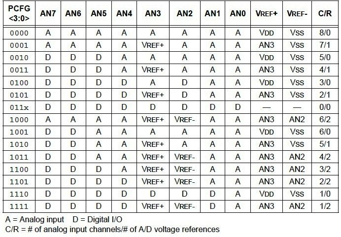
Note : Some ICs use special register ANSEL for setting each pin as analog or digital.
A/D Acquisition Time
Holding capacitor (CHOLD) must be charged to the input voltage to meet the accuracy specified by the datasheet. So we must provide a delay greater than the minimum required acquisition time to charge the capacitor. 19.72μs is the minimum time specified in the datasheet. Please refer the datasheet for more details.
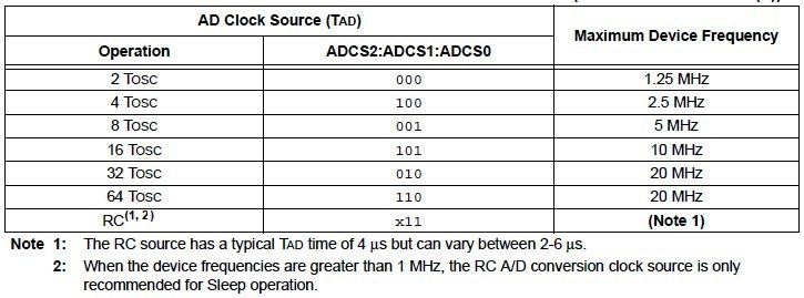
A/D Clock Selection
A/D conversion clock must be selected to ensure minimum TAD. TAD is the conversion time per bit, which is 1.6μs. Please refer the datasheet for more details.
Circuit Diagram
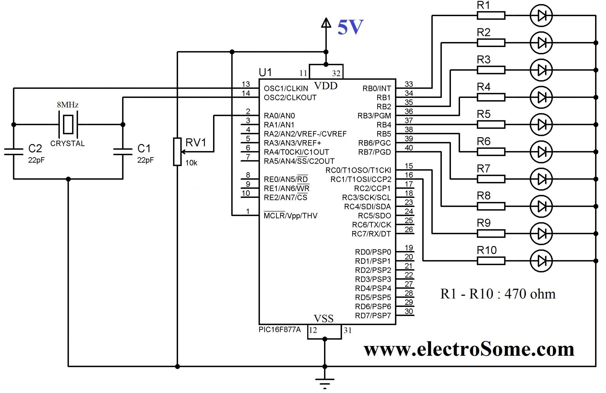
You can easily understand the circuit if you already go through our first tutorials, PIC Microcontroller MPLAB XC8 Tutorials. The reference voltages for A/D conversion is set to VDD (5V) and VSS (GND) in the software (see the code below). Analog input to Channel 0 is provided using a potentiometer such that we can vary the input voltage from 0 ~ 5V. A/D conversion will generate a 10 bit digital value (0 ~ 1023) corresponding to the analog input. This digital value is displayed using 10 LEDs connected PORTB and PORTC of the microcontroller.
MPLAB XC8 Code
// CONFIG
#pragma config FOSC = HS      // Oscillator Selection bits (HS oscillator)
#pragma config WDTE = OFF     // Watchdog Timer Enable bit (WDT disabled)
#pragma config PWRTE = OFF    // Power-up Timer Enable bit (PWRT disabled)
#pragma config BOREN = OFF    // Brown-out Reset Enable bit (BOR disabled)
#pragma config LVP = OFF      // Low-Voltage (Single-Supply) In-Circuit Serial Programming Enable bit (RB3 is digital I/O, HV on MCLR must be used for programming)
#pragma config CPD = OFF      // Data EEPROM Memory Code Protection bit (Data EEPROM code protection off)
#pragma config WRT = OFF      // Flash Program Memory Write Enable bits (Write protection off; all program memory may be written to by EECON control)
#pragma config CP = OFF       // Flash Program Memory Code Protection bit (Code protection off)

#include <xc.h>
#include <pic16f877a.h>

#define _XTAL_FREQ 8000000

void ADC_Init()
{
  ADCON0 = 0x81;               //Turn ON ADC and Clock Selection
  ADCON1 = 0x00;               //All pins as Analog Input and setting Reference Voltages
}

unsigned int ADC_Read(unsigned char channel)
{
  if(channel > 7)              //Channel range is 0 ~ 7
    return 0;

  ADCON0 &= 0xC5;              //Clearing channel selection bits
  ADCON0 |= channel<<3;        //Setting channel selection bits
  __delay_ms(2);               //Acquisition time to charge hold capacitor
  GO_nDONE = 1;                //Initializes A/D conversion
  while(GO_nDONE);             //Waiting for conversion to complete
  return ((ADRESH<<8)+ADRESL); //Return result
}

void main()
{
  unsigned int a;
  TRISA = 0xFF;                 //Analog pins as Input
  TRISB = 0x00;                 //Port B as Output
  TRISC = 0x00;                 //Port C as Output
  ADC_Init();                   //Initialize ADC

  do
  {
    a = ADC_Read(0);            //Read Analog Channel 0
    PORTB = a;                  //Write Lower bits to PORTB
    PORTC = a>>8;               //Write Higher 2 bits to PORTC
    __delay_ms(100);            //Delay
  }while(1);                    //Infinite Loop
}
I hope that the program is self explanatory as it is well commented.
Download Here
You can download the complete zipped project folder here.
I hope that you understand everything what I explained. Please do a comment if you have any doubt, which will help me to improve this tutorial.